As the computing power expansion of AI data centers drives CPO toward mass production, an overlooked link has become the bottleneck of the entire industrial chain, namely testing.
With the continuous scale expansion of AI data centers, traditional copper interconnects have approached their physical limits. Co-packaged Optics (CPO) is widely regarded by the industry as one of the critical interconnection solutions for next-generation AI infrastructure. TSMC’s COUPE platform is expected to enter mass production in 2026, marking CPO’s transition from laboratory R&D to commercialization.
Nevertheless, the inspection and testing of CPO remain an insurmountable barrier. The industry currently lacks unified standards and relies heavily on manual workflows, making testing a core constraint for the large-scale mass production of CPO chips. TrendForce has recently released a research report systematically analyzing this issue.
Why Is CPO Testing So Challenging?
To answer this question, it is essential to first understand CPO’s structural design.
CPO integrates optical components into Photonic Integrated Circuits (PIC), which are then co-packaged with Electronic Integrated Circuits (EIC) on a single chip. It replaces electrical circuits with optical paths to reduce power consumption and latency. The assembled component formed by PIC and EIC bonding is defined as the Optical Engine (OE).
Conventional EIC testing focuses purely on electrical performance, while PIC incorporates a wide range of optical components including couplers, modulators, photodetectors, optical filters and optical waveguides. The testing of a single OE requires comprehensive expertise in electricity, optics and optoelectronic interaction, resulting in far higher complexity than traditional semiconductor testing.
PIC testing needs to measure key parameters such as Insertion Loss (IL), Polarization Dependent Loss (PDL), responsivity, waveguide propagation loss and optical crosstalk, for which unified industry testing standards are yet to be established.
Another tangible physical challenge lies in the high-precision alignment of optical probes.
The process of transmitting external light from optical fibers into OE optical waveguides is defined as optical coupling. The core cross-sectional area of a single-mode optical fiber is approximately 78.5 square micrometers, while that of an optical waveguide is merely 0.099 square micrometers, a gap of nearly 800 times. Without nanometer-level alignment accuracy, extreme coupling loss will be inevitable.
It requires the fiber array to maintain a precise distance from the surface of wafers and chips, while fine-tuning the angle of couplers to maximize optical power transmission and scan across multiple wavelength bands in sequence. Currently, most of these operations still depend on manual intervention.
Consequently, the 100% full inspection of a single PIC chip takes over 100 seconds on average, becoming one of the core bottlenecks restricting high-volume CPO production.
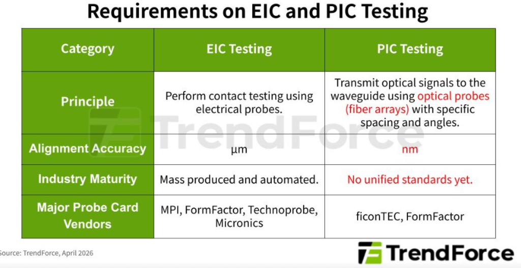
EIC vs. PIC Testing Comparison Chart — covering four dimensions: testing principles, alignment accuracy, industry maturity and major probe card manufacturers. Source: TrendForce (same below).
Which Stage Matters Most Among the Four Testing Phases?
A complete CPO chip lifecycle, from wafer fabrication to system integration, involves four core testing phases:
Phase 1: PIC Wafer-Level Optical Testing (OWAT)
Basic DC electrical and optical testing, including the measurement of core optical parameters such as optical power, loss and dark current.
Phase 2: EIC-PIC Co-Wafer Testing
Modulation function testing (electro-optic, opto-electric and optical-optical), high-speed performance testing and S-parameter measurement.
Phase 3: OE-Level Testing
Full-process calibration, DC testing, high-speed testing, optical loop testing and S-parameter measurement. This is the critical phase to identify Known Good Optical Engines (KGOE).
Phase 4: Advanced Packaging Module-Level Testing
Full-system functional verification and optical loop validation.
Among the four phases, PIC wafer-level optical testing in Phase 1 carries the highest priority.
The logic is straightforward: PICs are generally manufactured with mature process nodes, whereas EICs adopt advanced and high-cost processes. Screening out defective PICs at the wafer stage prior to EIC bonding can avoid wasting high-value EIC chips on faulty photonic components, and substantially cut losses in subsequent production processes.
It is identical to assembly line quality inspection: defect detection at an earlier stage always minimizes operational losses.
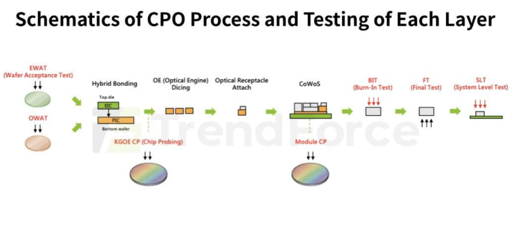
CPO Manufacturing Process and Testing Phase Schematic — full-process flowchart from incoming wafer inspection to system-level testing.
Equipment Market Landscape: Traditional Giants Upgrade, New Players Emerge
The CPO test equipment market is rapidly taking shape, with industrial integration between mainstream Automatic Test Equipment (ATE) giants and professional optical testing vendors as the core development trend.
Advantest & FormFactor
The global EIC testing market is long dominated by Japan’s Advantest and the United States’ Teradyne. As CPO testing demands dual capabilities in EIC and PIC validation, both giants have partnered with professional optical probe suppliers to reinforce their optical technology shortcomings.
Advantest has chosen strategic cooperation with FormFactor. In June 2024, Advantest jointly launched the UFO probe card with Jenoptik and Ayar Labs, integrating electrical and optical probes into a single card to realize synchronous electro-optical testing. Its core innovation is alignment tolerance compensation technology, which shapes the output beam of optical probes in a customized manner. Even with minor positioning deviations, optical signals can still be effectively coupled into PIC couplers, greatly shortening alignment time.
In April 2025, Advantest and FormFactor further released the V93000-Triton photonic testing system, equipped with 9-axis photon alignment functions and FormFactor’s OptoVue Pro optical alignment system. The proprietary CalVue technology adopts uniquely designed retroreflective mirrors to monitor fiber arrays, and leverages machine vision algorithms to calibrate Z-axis displacement and optical positioning in real time, further optimizing fiber alignment efficiency.
Teradyne & ficonTEC
Teradyne has adopted a dual strategy of mergers & acquisitions plus industrial collaboration. In 2025, Teradyne acquired Quantifi Photonics and established a partnership with Germany-based ficonTEC, currently a subsidiary of China’s Robotechnik.
In March 2025, the two parties jointly unveiled the industry’s first high-yield 300mm dual-sided wafer probe testing system. ficonTEC provides the WLT-D2 dual-sided wafer testing platform with 50-nanometer high-precision alignment, enabling concurrent electrical testing on the wafer top and optical testing on the wafer bottom to boost overall testing efficiency. Teradyne supplies the UltraFLEXplus ATE platform and IG-XL system software.
The subsequently launched DLT-D1 dual-sided chip-level testing system supports up to three parallel test heads to improve throughput and reduce unit testing costs. To date, ficonTEC has built a comprehensive CPO testing product portfolio covering wafer-level to chip-level solutions.
Keysight
As a global leader in precision measurement instruments, Keysight delivers complete PIC wafer testing solutions with seamless integration with FormFactor and full compatibility with FormFactor’s Velox probe control software.
Keysight’s N778x series polarization synthesizers enable rapid switching among multiple States of Polarization (SOP). Combined with the N7700100C Polarization Lambda scanning software, it calculates critical metrics including IL, PDL and TE/TM IL through matrix algorithms. This solution eliminates the need for polarization-maintaining fibers and manual polarization correction at multiple wavelength points, significantly improving testing efficiency. Its exclusive SOP stabilization technology locks the input light polarization at fixed coordinates, ensuring stable optical coupling throughout full-band wavelength scanning.
Chroma
Chroma is a worldwide leader in System-Level Testing (SLT) equipment. Its photodiode aging and reliability testing system, the Model 58604 / 58604-C / 58606 series, is specially developed for the reliability validation of 3D sensors, lasers, photodetectors, modulators and other core PIC components. The Model 58606 provides 256 SMU channels per layer, with support for up to 7 layers and a total of 1,792 channels. Chroma has announced plans to leverage its mature SLT optical testing expertise to accelerate R&D in CPO-dedicated test equipment.
Enlitech
In September 2025, Enlitech collaborated with iST to launch the Night Jar silicon photonic chip testing platform. As an add-on hyperspectral imaging and analysis system, it is compatible with probe stations of all brands and applicable to WAT, CP, FT and other mainstream testing stages.
Night Jar addresses a long-standing industry pain point. Previously, leaky light positions inside optical waveguides could only be roughly estimated via reflected light, with only overall or average optical loss data available. The Night Jar system can accurately locate light leakage points, quantify the Insertion Loss of specific waveguide segments and optical components, and support wafer-level optical loss mapping. It helps R&D teams identify defects efficiently and ultimately improve production yield.
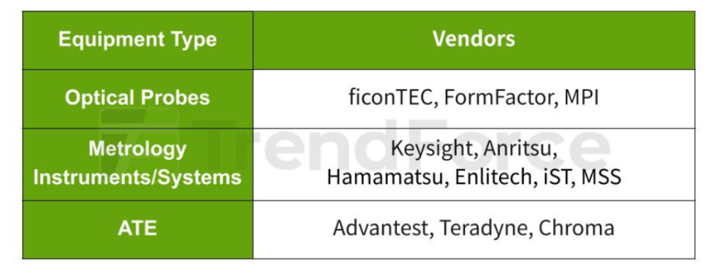
CPO Test Equipment Supply Chain Panorama — supplier distribution covering three major categories: optical probes, metering instruments & systems, and automatic test equipment.
Expanding Market Opportunities Lie Ahead
With semiconductor chip designs becoming increasingly sophisticated, SoC testing difficulty continues to rise. The number of test stations required for single chips and overall testing duration keep growing, driving up the proportion of test equipment in semiconductor capital expenditure. The proportion is projected to climb further as CPO chips are widely deployed.
The CPO test equipment market is taking shape rapidly. In terms of competitive landscape, leading ATE vendors including Advantest and Teradyne are rapidly strengthening their optical capabilities through mergers, acquisitions and strategic cooperation, while Keysight, Chroma, Enlitech and other specialized suppliers consolidate their advantages in segmented tracks. The entire industrial supply chain, ranging from optical probes and precision metering instruments to high-end automatic test equipment, is being restructured to meet the booming market demand for CPO testing.
Comments