Since July, the AI trade that had been leading U.S. equity markets sharply higher has suddenly cooled.
The catalyst came partly from profit-taking in richly valued technology stocks, and partly from the approaching earnings season, which prompted the market to reassess AI return on investment. After a rapid rally in the first half of the year, chip, memory, and AI infrastructure stocks experienced pronounced volatility. The Philadelphia Semiconductor Index retreated from its highs, and Micron, AMD, Intel, and several equipment stocks all suffered significant declines at various points. The market's key concern has also shifted: investors are no longer simply asking how much more AI demand can grow. Instead, they are beginning to re-examine whether high valuations can be justified by future earnings, whether cloud-provider capital expenditure will continue its rapid expansion, and whether profitability across the supply chain can keep pace with stock prices.
But this does not mean the AI investment cycle is over.
On the contrary, the current moment looks more like a transition — from buying everything with an AI label to searching for genuine orders and real earnings. In the previous phase, the market was willing to pay a premium for speculative potential; entering the earnings-verification period, investors care more about who can consistently win orders, who possesses irreplaceable technical moats, and whose revenue does not depend entirely on a single chip or a single customer.
Against this backdrop, semiconductor equipment companies such as Applied Materials, Lam Research, and KLA are re-entering investors' field of vision.
Equipment stocks have also pulled back, and their near-term performance is not necessarily more stable than that of chip design companies. It is therefore inaccurate to describe them simply as the new theme toward which capital has already rotated. The more worthwhile question is this: as the AI industry moves from a GPU shortage toward a broad capacity build-out across memory, advanced process nodes, and advanced packaging, is the earnings visibility of equipment companies improving? Can Micron's expanded U.S. investment, SK Hynix's HBM advanced packaging hub in Indiana, and the rising capital expenditure of global memory makers turn equipment stocks into more durable beneficiaries in the next phase of the AI investment cycle?
From Buying Chips to Building Capacity
Over the past three years, the most visible investment opportunities in the AI industry have been concentrated in the chip design segment.
NVIDIA became the biggest winner thanks to its GPU and CUDA ecosystem; Broadcom benefited from custom AI chips; AMD competed for market share with its accelerator products. Chip design companies directly captured the growth in AI server demand, with high revenue elasticity — making them the easiest to attract market attention.
But the high growth of chip design companies does not mean the entire supply chain has sufficient production capacity.
A single AI accelerator, from completed design to deployment in a data center, must pass through wafer fabrication, etching, deposition, cleaning, inspection, memory integration, packaging, and testing. The more intense the demand for compute, the higher the requirements for advanced logic process nodes, HBM, advanced packaging, and inspection equipment.
The first phase of AI investment was cloud providers competing for GPUs; the second phase is the entire semiconductor supply chain expanding capacity around AI demand.
The fundamental difference between the two is that the former was largely reflected in the sales volume and pricing of a single product, while the latter translates into multi-year capital expenditure by wafer fabs. Once TSMC, Micron, SK Hynix, Samsung, or Intel decides to build a new fab, upgrade a process node, or expand HBM capacity, it must procure large volumes of equipment in advance. The construction and qualification cycle for a wafer fab is very long, and once equipment is installed it also involves ongoing maintenance, spare-parts replacement, and process upgrades. For equipment vendors, a single capacity expansion cycle represents not only a one-time equipment sale but potentially years of recurring service revenue.
This is the key differentiating characteristic of equipment stocks relative to some chip design companies: they do not bet on which single AI chip ultimately wins. They sell tools to every manufacturer that wants to expand its advanced production capacity. Whether the chips that ultimately capture more market share are NVIDIA GPUs, Google TPUs, Amazon Trainium, or other custom ASICs, as long as these chips require more advanced process nodes, more complex transistor structures, higher-bandwidth memory, and more precise packaging, equipment demand will increase.
SEMI's latest Total Semiconductor Equipment Forecast (OEM Perspective) projects that the global semiconductor equipment market will continue growing in the coming years, with 2026 sales forecast at $165.9 billion, up 23.2% year-over-year; rising further to $201.2 billion in 2027 and potentially reaching $229.5 billion in 2028. At the same time, SEMI projects that 2026 global 300mm memory wafer fab equipment investment will exceed $50 billion for the first time, reaching $52 billion, with DRAM equipment spending up 29% to $37 billion and 3D NAND equipment spending up 28% to $14 billion, primarily driven by HBM and DDR5 demand. This shows that despite the recent AI sector pullback, capital expenditure on the semiconductor manufacturing side continues to expand.
The market is shifting from "whose GPU sells best" to "who can most sustainably benefit from AI capital expenditure." Compared to chip design companies that rely on a single product cycle, equipment companies face demand from the expansion of the entire manufacturing system. Their demand sources are therefore more diversified, and their financial performance is easier to track through customer capital expenditure, delivery schedules, and service revenue — this is the core logic behind capital's renewed attention to the equipment sector.
Why HBM Demands Far More Equipment Than Conventional Memory
One of the most important incremental drivers for the semiconductor equipment sector today is HBM.
In a conventional server, the computational bottleneck is primarily determined by processor performance. But AI models require rapid transfer of massive amounts of data between processor and memory. Compared to conventional DDR or GDDR memory solutions, HBM vertically stacks multiple DRAM dies and combines TSV (Through-Silicon Via) and advanced packaging technology to deliver higher bandwidth, lower power consumption, and a smaller package footprint. It has therefore become the mainstream memory solution for high-end AI accelerators.
The value of HBM lies not only in its higher selling price, but also in its substantially greater manufacturing difficulty compared to standard DRAM.
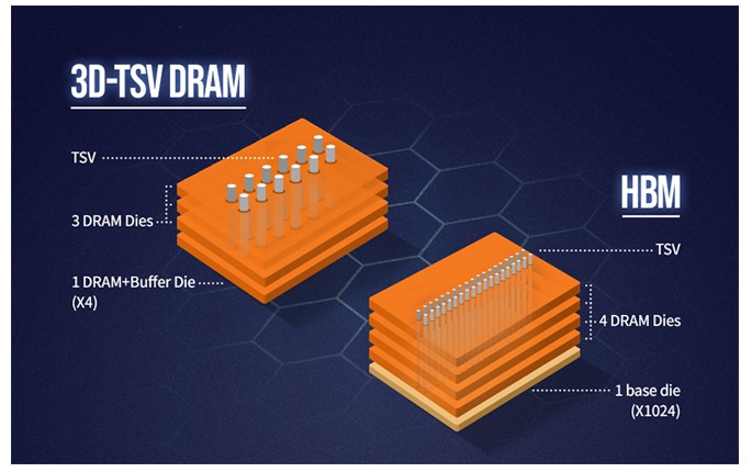
Source:SK Hynix
First, HBM consumes far more wafer area than conventional DRAM. HBM's consumption of front-end DRAM capacity is significantly higher than that of traditional DDR products. Based on public statements from Micron, SK Hynix, and other manufacturers, the front-end capacity consumed per unit of HBM output is typically approximately 2–3 times that of a conventional DDR product, though the actual ratio varies with product generation, die area, stack count, and yield. As a result, memory makers looking to expand HBM shipments generally cannot rely solely on adjusting their product mix — they must also increase front-end DRAM capacity in parallel. According to TrendForce's June 2026 forecast, the share of HBM wafer starts in total DRAM wafer starts at the three major memory suppliers (Samsung, SK Hynix, and Micron) is expected to reach approximately 18%, 22%, and 30% at year-end 2025, 2026, and 2027, respectively. As HBM's share continues to rise, its multiplier effect on front-end capacity and equipment investment will grow more pronounced.
Second, HBM stack counts are continuously increasing. As HBM evolves toward higher stack counts, greater bandwidth, and larger capacity, overall requirements across wafer thinning, TSV, bonding, thermal management, inspection, and yield control continue to rise. However, different suppliers adopt different packaging processes and bonding approaches, so specific technical implementations vary.
Third, HBM does not only require front-end manufacturing equipment. After wafer completion, advanced packaging, inspection, and testing are still required. As stack counts increase, the importance of process control grows, and equipment for inspection, metrology, bonding, and testing also benefits.
This means that HBM capacity expansion will benefit not just memory manufacturers — it also channels capital expenditure into etching, deposition, cleaning, inspection, metrology, bonding, and testing equipment.
Micron projects that the total HBM market will grow from approximately $35 billion in 2025 to approximately $100 billion in 2028, implying a CAGR of approximately 40%. The company has already completed price and volume agreements covering its entire 2026 HBM supply.
Demand has been locked in. The next step is converting orders into capacity — and that is the direct source of equipment demand.
Micron's U.S. Investment Is Scaling to a New Level
Micron's U.S. capacity expansion plan is one of the most direct windows through which to observe equipment demand.
Micron has most recently raised its expected total U.S. wafer fab and technology project investment through 2035 to more than $250 billion. Previously disclosed plans cover advanced memory fabs in Idaho and New York, a facility upgrade in Virginia, U.S. R&D capabilities, and advanced HBM packaging capacity — though the specific allocation of the newly announced incremental funding has not been detailed line by line. The company aims to establish approximately 40% of its DRAM capacity in the United States over the long term.
More recently, Micron announced a further step to strengthen its domestic supply chain. On July 9, 2026, Micron announced a proposed $500 million strategic financing commitment to GlobalWafers' 300mm prime silicon wafer project in Sherman, Texas, along with a planned 10-year supply agreement. The proposed transaction remains subject to the execution of definitive agreements and satisfaction of customary closing conditions. If completed, this partnership would help Micron lock in the critical silicon wafer supply needed for its advanced U.S. memory capacity expansion. The logic is not simply to purchase more raw materials — it is to pre-secure key upstream resources required for AI memory expansion.
For the equipment industry, Micron's investment will generate demand on at least three levels:
The first level is greenfield fab construction. A single advanced memory fab requires the procurement of large quantities of deposition, etching, cleaning, and inspection equipment. The more complex the layer count and structure of the memory chip, the more times each wafer passes through equipment, and the higher the equipment investment per unit of capacity.
The second level is process upgrades. Even without building entirely new facilities, Micron must update existing production lines to improve HBM performance and yield. Equipment companies therefore benefit not only from capacity growth but also from process changes.
The third level is advanced packaging. Micron has explicitly included end-to-end HBM packaging capability in its U.S. investment plan. HBM packaging involves bonding, wafer thinning, inspection, and materials handling across multiple steps — extending the investment scope from traditional wafer fabrication into the back end.
Micron's capacity expansion therefore does not simply mean adding a few factories. It represents the United States' attempt to complete the entire supply chain from silicon wafers, through memory fabrication, to HBM packaging.
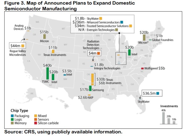
Source:Congress Research Service
SK Hynix Is Also Building in the U.S. — But Not a Conventional Wafer Fab
SK Hynix plans to invest approximately $3.87 billion in West Lafayette, Indiana. The company describes the project as the first dedicated AI-product facility in the United States to integrate HBM advanced packaging manufacturing and R&D under one roof. The project is planned to include HBM-related production lines and advanced packaging R&D facilities, with mass production targeted to begin in the second half of 2028. The core of the project is not to relocate all of SK Hynix's DRAM wafer fabrication to the United States — it is to bring HBM stacking, packaging, and R&D capabilities to U.S. soil.
SK Hynix's DRAM front-end manufacturing is distributed across production bases in Icheon and Cheongju in South Korea, as well as its Wuxi factory in China. The Indiana project is not a DRAM front-end wafer fab; rather, it focuses on next-generation HBM advanced packaging manufacturing and related R&D, stacking and packaging the DRAM dies completed in front-end fabrication, and integrating them with AI processors into high-bandwidth memory systems.
This distinction matters enormously.
Describing the project simply as SK Hynix building an HBM wafer fab in the U.S. would overstate its direct contribution to America's front-end equipment market. But viewed through a supply chain lens, the project remains significant: the reshoring of U.S. semiconductors is extending from wafer fabrication into advanced packaging — and packaging is one of the tightest and most rapidly evolving segments of the AI chip supply chain.
Historically, the United States has held advantages in chip design and semiconductor equipment, but large volumes of manufacturing and packaging capacity have been concentrated in Asia. Fabricating wafers only in the United States while still shipping chips to Asia for packaging cannot constitute a complete domestic supply chain. SK Hynix's Indiana project, Micron's U.S. HBM packaging plan, and other packaging investments signal that policy and industrial capital are beginning to close this gap.
This opens a new market for equipment vendors.
Traditionally, when investors discussed equipment stocks, they focused mainly on front-end wafer fabrication equipment. Going forward, as Chiplet, HBM, and heterogeneous integration become mainstream, the boundary between front-end manufacturing and back-end packaging is blurring. Packaging processes are beginning to employ more equipment and precision control approaching wafer fabrication standards, and equipment companies' serviceable addressable market is expanding accordingly.
Three Core Beneficiary Stocks: Financial Data and Investment Thesis
Applied Materials: The Most Diversified "Picks and Shovels" Provider
Applied Materials is one of the broadest-coverage companies in this investment thesis, with products spanning deposition, materials engineering, ion implantation, planarization, inspection, and packaging, among other areas. Compared to vendors focused on a single equipment category, Applied Materials can simultaneously benefit from advanced logic, DRAM, NAND, and advanced packaging investment.
AI chip advancement can no longer rely solely on transistor shrinkage. As process nodes approach physical limits, chip companies are improving performance through new materials, backside power delivery, gate-all-around transistors, Chiplet architectures, and advanced packaging. These changes increase the complexity of materials engineering and imply more deposition, etching, and precision processing steps.
For Applied Materials, the value of AI is not merely that customers build more factories — it is that each advanced wafer requires more equipment.
Applied Materials reported revenue of $7.91 billion in fiscal Q2 2026, up 11% year-over-year, with adjusted earnings per share up 20% year-over-year; both revenue and earnings set new records for the period. The company guides for next-quarter revenue to reach a midpoint of $8.95 billion, continuing to grow sequentially. Management projects semiconductor equipment business growth of more than 30% for calendar year 2026. From a revenue mix perspective, the DRAM revenue share increased further, with advanced logic, HBM, and advanced packaging as the primary growth drivers. The Applied Global Services segment, which covers spare parts, services, and equipment upgrades, grew revenue approximately 17% year-over-year. As the installed base grows, this segment supports revenue durability and helps cushion the cyclical swings of new equipment sales to some degree.
Applied Materials' advantage lies in its diversification and broad product line, giving it comprehensive exposure to AI capital expenditure. However, this also means the company is not the purest HBM investment vehicle. Its performance will still be affected by mature process nodes, display equipment, regional demand, and export restrictions. When evaluating Applied Materials, one should look beyond the AI narrative to track semiconductor systems revenue growth, advanced packaging-related revenue, DRAM customer spending, and whether the services business can continue expanding steadily.
Lam Research: High-Elasticity Beneficiary of Memory Capacity Expansion
Compared to Applied Materials, Lam Research has a tighter linkage to memory capital expenditure. Lam's core strengths lie in etching, deposition, and cleaning equipment. Whether NAND is adding layers or DRAM is evolving to more advanced structures, both require more precision etching and thin-film deposition steps.
HBM demand growth creates a two-pronged tailwind for Lam.
On one side, HBM requires more advanced DRAM capacity. As Micron, SK Hynix, and Samsung expand HBM output, front-end equipment spending increases. On the other side, as memory structures grow more complex, the number of equipment process steps per wafer increases. Even if the industry's new wafer capacity does not grow in direct proportion, the equipment investment per unit wafer may still rise.
For the quarter ended March 2026, Lam Research reported revenue of $5.841 billion, up approximately 24% year-over-year, with gross margin improving to 49.8% and operating margin reaching 35%, reflecting continued earnings quality improvement. The company guides for next-quarter revenue to rise further to a midpoint of $6.6 billion, with GAAP and Non-GAAP gross margin guidance midpoints both at 50.5%, corresponding to a guidance range of approximately 49.5%–51.5%. Lam's etching, deposition, and cleaning businesses have high sensitivity to DRAM, NAND, and HBM-related memory capital expenditure. As Micron, SK Hynix, and Samsung continue expanding HBM capacity, the company stands to benefit directly from memory capex growth.
Lam is also among the more cyclically elastic companies in the equipment space. When memory makers significantly raise capital expenditure, Lam tends to benefit rapidly; but when memory prices fall and manufacturers cut investment, its earnings can also face more pronounced pressure. The investment thesis for Lam therefore requires simultaneous attention to HBM demand and the traditional DRAM and NAND cycle.
If memory makers concentrate capital solely on HBM while constraining supply of conventional DRAM and NAND to support prices, Lam can still benefit — but the magnitude depends on whether HBM investment can offset the volatility in conventional memory equipment spending.
KLA: The Higher the Yield Challenge, the Greater the Inspection Value
KLA's most significant difference from Applied Materials and Lam is that it does not primarily participate in materials processing. Instead, it helps wafer fabs find defects, measure process deviations, and improve yield.
Inspection was already an essential step in mature process nodes; its importance increases further as chips advance to the leading edge and into the HBM era.
Advanced chip production carries extremely high costs. After a wafer passes through hundreds of process steps, discovering a defect late in the flow wastes all the manufacturing costs invested up to that point. The more complex the process node, the more willing wafer fabs are to increase inspection in order to detect problems earlier.
HBM amplifies this need further. A defect in a single DRAM die may impact not just that chip, but the entire stacked assembly. As HBM stack counts increase and packaging structures become more complex, requirements for defect inspection, overlay accuracy, and packaging inspection all rise.
KLA therefore possesses a relatively distinctive characteristic: it benefits not only from capacity expansion, but also from the increasing difficulty of yield management. KLA's business model typically features high gross margins and strong service revenue, but the market also tends to assign it a higher valuation premium. KLA is therefore not necessarily the cheapest equipment stock on a valuation basis. If the market continues to de-rate high-valued technology stocks, KLA may also be affected. Its earnings certainty derives more from technological moats and yield-control requirements.
For the quarter ended March 2026, KLA reported revenue of $3.42 billion, up approximately 11% year-over-year, exceeding the company's prior guidance midpoint. The company guides for next-quarter revenue to continue growing to approximately $3.58 billion. Compared to Applied Materials and Lam, KLA's greatest advantage lies not in revenue elasticity but in earnings quality: Non-GAAP gross margin is expected to approach 62%, leading among large-cap semiconductor equipment companies. As AI chip process nodes become ever more complex and HBM stack counts continue to rise, wafer fabs' dependence on inspection and metrology equipment deepens. KLA benefits not only from capacity expansion but from the growing requirement for yield control in advanced processes. The company maintains consistently high gross margins and strong free cash flow generation; at the same time, its process control business carries high technological barriers, enabling it to sustain a strong competitive position as advanced process nodes and advanced packaging continue to evolve.
Valuation Snapshot
After a significant rally in the first half of 2026, the valuations of all three companies already reflect a substantial portion of AI manufacturing expansion expectations. KLA typically commands a premium for its process control moat, high gross margins, and cash flow quality. Lam's valuation is more sensitive to the memory capex cycle. Applied Materials, with its broader product coverage, exhibits a relatively balanced earnings profile.
Company | Forward P/E | Earnings Profile | Typical Valuation Premium Source | Key Risk |
AMAT | 39.9x | Broadest product coverage, most diversified business | Integrated platform capabilities and multi-line exposure across advanced logic, memory, and packaging | Diversification also dilutes HBM purity |
LRCX | 45.7x | Higher sensitivity to DRAM, NAND, and HBM investment | Earnings elasticity in memory upcycles | Memory capex downturn |
KLA | 48x | Leading gross margins and cash flow quality | Process control moat, software capabilities, and service revenue | High valuation premium, sensitive to de-rating |
Data Source: StockAnalysis
Why Equipment Stocks Cannot Simply Be Labeled "Safer"
The industrial logic for equipment companies is strengthening — but this does not mean equipment stocks are without risk.
The first risk is the cyclicality of capital expenditure. Semiconductor equipment orders typically lead wafer fab capacity additions. If customers are overly optimistic about future demand and rush to expand capacity together, oversupply may follow. Once memory prices fall or cloud providers reduce AI investment, wafer fabs swiftly cut equipment budgets. Equipment companies' order visibility is generally better than that of some chip design firms, but their cyclical volatility has not disappeared.
The second risk is that HBM capacity expansion could alter supply-demand dynamics. HBM supply is currently tight, and memory makers hold relatively strong pricing power. As Micron, SK Hynix, and Samsung continue expanding, the pace of supply growth could accelerate. If AI demand growth disappoints, HBM could shift from scarcity to a phase of oversupply. Equipment vendors typically benefit first from an expansion cycle, but they may also be the first to feel the effects of capital expenditure peaking.
The third risk is export restrictions. U.S. equipment companies derive a meaningful share of revenue from Asia, and particularly from China. Escalating export controls could restrict the shipment of certain advanced equipment, while customers' front-loading of purchases could cause quarterly revenue volatility. Investors cannot focus only on orders from new U.S. fabs while ignoring changes in global market structure.
The fourth risk is valuation. Equipment stocks also experienced substantial gains in the first half of 2026 and are not traditional low-valuation defensive holdings. KLA, Lam, and Applied Materials have all seen sharp declines at various points, indicating that when the market deleverages or reduces its technology exposure, equipment stocks will not be immune.
The concept of "certainty" in this context does not mean share prices can only rise — it means the growth thesis can be verified through customer capital expenditure, equipment orders, revenue, and margins.
What to Watch in the Next Phase
Whether semiconductor equipment stocks can truly become the dominant theme of the next AI market phase depends less on near-term share prices than on whether several leading industry indicators continue trending positively.
First: whether memory manufacturers' capital expenditure continues to be revised upward. This indicator is currently still in an uptrend. Micron has raised its U.S. investment plan to more than $250 billion, SK Hynix continues expanding HBM capacity and is advancing its U.S. advanced packaging hub, and TrendForce projects the HBM share of the three major memory suppliers' DRAM wafer starts will rise from approximately 18% at end-2025 to approximately 22% at end-2026. If Samsung, SK Hynix, and Micron continue raising HBM-related capital expenditure rather than reverting to conventional DRAM or NAND expansion, it suggests equipment demand remains durable.
Second: whether AI infrastructure investment slows. The market's most important support continues to come from large cloud providers. S&P Global Ratings projects that the combined capital expenditure of five U.S. hyperscalers — Microsoft, Amazon, Alphabet, Meta, and Oracle — will exceed $700 billion in 2026, up more than 60% year-over-year. To date, none has signaled a clear intention to cut AI infrastructure investment. AI data centers, servers, and network infrastructure remain the focal points of capex. Based on the latest earnings and management guidance, all five companies continue to maintain elevated AI infrastructure investment intensity without clear signals of downward revision — this remains one of the most important support factors for semiconductor equipment demand.
Third: whether equipment companies' orders continue to be fulfilled. Based on the latest earnings, Applied Materials, Lam Research, and KLA have all issued guidance for continued revenue growth, indicating that AI demand is already converting into equipment deliveries. What truly requires monitoring is whether these revenue guidance figures can continue to be revised upward over the next several quarters, and whether gross margins, deferred revenue, and cash flow improve in tandem. If revenue growth begins to decelerate while orders and margins simultaneously weaken, it would suggest the current equipment investment cycle may be entering a plateau.
Fourth: whether advanced packaging becomes the new center of capital expenditure. Equipment demand is no longer confined to front-end wafer fabrication. Micron is building HBM packaging capability in the United States; SK Hynix is constructing an advanced packaging hub. This signals that capital expenditure has begun extending toward the back end. If CoWoS, HBM, Chiplet, and other advanced packaging investments continue to increase, it would mean the AI manufacturing chain is still expanding, and equipment companies' serviceable addressable market could grow further.
Will Equipment Stocks Become the Next AI Theme?
From an industry trend perspective, the answer leans toward yes. From a trading perspective, earnings confirmation is still needed.
AI infrastructure buildout is diffusing from a handful of GPU vendors to the entire manufacturing chain. Advanced logic, HBM, advanced packaging, and domestic supply chains all require more semiconductor equipment. Micron's large-scale U.S. DRAM and HBM capacity expansion, SK Hynix's advanced packaging hub in Indiana, and TSMC and other fabs' continued investment in advanced capacity have already provided the equipment industry with a medium-to-long-term demand foundation.
Compared to companies that rely solely on a single product cycle, Applied Materials, Lam Research, and KLA can simultaneously serve multiple wafer fabs and multiple technology roadmaps. As competition in AI chips moves from one-player dominance toward coexistence among GPUs, ASICs, and custom silicon, equipment vendors could paradoxically become the shared beneficiaries of them all.
But the market has not completed a clear rotation from chip design stocks to equipment stocks. Equipment stocks themselves experienced significant volatility during July's selloff — indicating that capital is still reassessing the entire semiconductor sector, rather than simply migrating from one sub-segment to another.
The more accurate assessment is therefore this: semiconductor equipment stocks are transitioning from supporting actors in the AI rally into a direction that must be closely tracked in the next phase.
Their appeal does not lie in near-term defensive qualities, but in the fact that AI industry capital expenditure is entering a heavier, longer, and more irreversible manufacturing phase. GPU orders can shift rapidly with product cycles. A wafer fab, an HBM production line, or an advanced packaging hub — once construction begins — typically requires continuous equipment investment over many years.
The earlier phase of the AI trade was trading scarcity of computing power. In the next phase, the market may be trading scarcity of manufacturing capacity.
And in the process of expanding manufacturing capacity, the entities that can continuously monetize across different chip architectures, different customers, and different product cycles — are precisely those companies that master the core technologies of etching, deposition, inspection, and materials engineering: the picks-and-shovels providers.
Whether semiconductor equipment stocks can become the next major theme ultimately depends on two questions: whether AI demand can continue converting into wafer fab capital expenditure, and whether equipment companies' profit growth can match market expectations.
For now, the first condition is forming. The second will be answered by the next several rounds of earnings reports.
Disclaimer: This article is for informational purposes only and does not constitute investment advice. All investments involve risk; please invest responsibly.
Find out more
Comments