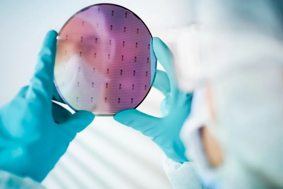
擴產能,降成本!意法半導體制造首批200mm碳化硅晶圓
意法半導體(簡稱ST)今天宣佈,ST瑞典北雪平工廠製造出首批200mm (8寸)碳化硅(SiC)晶圓片,這些晶圓將用於生產下一代電力電子芯片的產品原型。SiC晶圓升級到200mm標誌着ST面向汽車和工業客戶的擴產計劃取得重要的階段性成功,鞏固了ST在這一開創性技術領域的領導地位,提高了電力電子芯片的輕量化和能效,降低客戶獲取這些產品的總擁有成本。
意法半導體先進的量產碳化硅產品STPOWER SiC目前是在卡塔尼亞(意大利)和宏茂橋(新加坡)兩家150mm晶圓廠完成前工序製造,後工序製造是在深圳(中國)和布斯庫拉(摩洛哥)的兩家封測廠進行的。這個階段性成功是意法半導體佈局更先進的、高成本效益的200mm SiC量產計劃的組成部分。SiC晶圓升級到200mm屬於公司正在執行的SiC襯底建新廠和內部採購SiC襯底佔比超40%的生產計劃。
來源:ST
Disclaimer: Investing carries risk. This is not financial advice. The above content should not be regarded as an offer, recommendation, or solicitation on acquiring or disposing of any financial products, any associated discussions, comments, or posts by author or other users should not be considered as such either. It is solely for general information purpose only, which does not consider your own investment objectives, financial situations or needs. TTM assumes no responsibility or warranty for the accuracy and completeness of the information, investors should do their own research and may seek professional advice before investing.
- edwardkoh626·2021-08-03Bigger SIC wafers mean reduce cost per dice.LikeReport


